This post, final in the pair of posts, describes Lokawiz RTL IP Prototype setup. The first post in this series is available at Part I. This post (Part II) finally describes the internal connection of IP Cores inside the FPGA in ProASIC3 Starter Kit from Microsemi. Furthermore, it also demos FPGA flashing with Libero and a sample running setup.
Background
Lokawiz has very good expertise with RTL development and verification. We specialize in end-to-end embedded solutions from concept till final production. We have some very high quality RTL IP cores which are ready to plug and play in bigger RTL systems design. These IP cores can also be very easily customized based on system integration requirement of the top level RTL setup. Following is the list of our IP cores along with their description page links.
RTL IP Connections
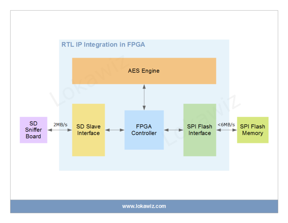
The featured image describes the RTL IP connections inside the FPGA in ProASIC3 Starter Kit from Microsemi. An SPI Sniffer board from SparkFun connects to the Starter Kit to enable SD operations. In addition, a breakout board mounted with Winbond SPI flash also connects to the Starter Kit for memory operation.

The FPGA Controller controls the flow of data between SD card and the SPI flash memory. Furthermore, it uses the AES Engine to encrypt and decrypt the data. The SPI Flash memory contains the encrypted data whereas SD Card contains normal data readable by a computer machine. For the Starter Kit, the data flow works at 2MB/s at SD side interface and at less than 6MB/s at SPI side interface.
The data flows in both the directions are described below:
SD Card to SPI Flash
First of all, the SD Slave Interface reads data from SD Card through SD Sniffer Board. Then the FPGA Controller uses AES Engine to encrypt this data. Finally, SPI Flash Interface writes the encrypted data into SPI Flash memory.
SPI Flash to SD Card
The data flow in this direction goes as follows. First of all, SPI Flash Interface reads the encrypted data from SPI Flash memory. Then, FPGA controller uses AES Engine to decrypt the encrypted data. Finally, SD Slave Interface writes the data into SD Card the the Sniffer Board.
Programming FPGA with RTL IP build
The following video demos how to burn the FPGA with the build containing RTL IPs. We used FlashPro4 and Libero software to flash the FPGA on the ProASIC3 Kit.
Prototype Setup Run
The following video demos a sample run for the prototype and evaluation setup. In this video please observe that the SD Sniffer board is soldered to ProASIC3 board. This was necessary to avoid the signal integrity issue which we faced with board connection using connecting wires as shown in Part I setup demo video.